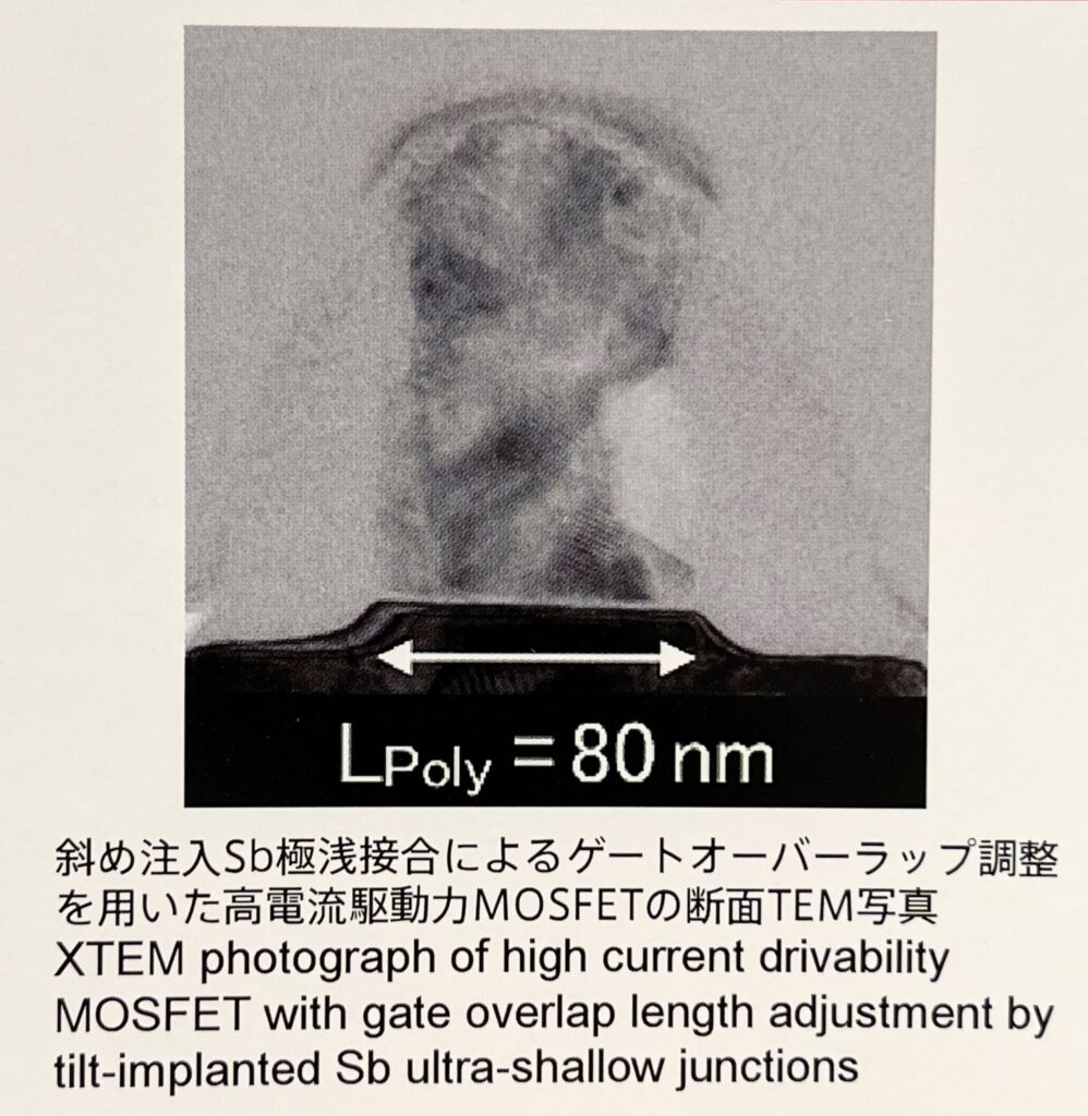
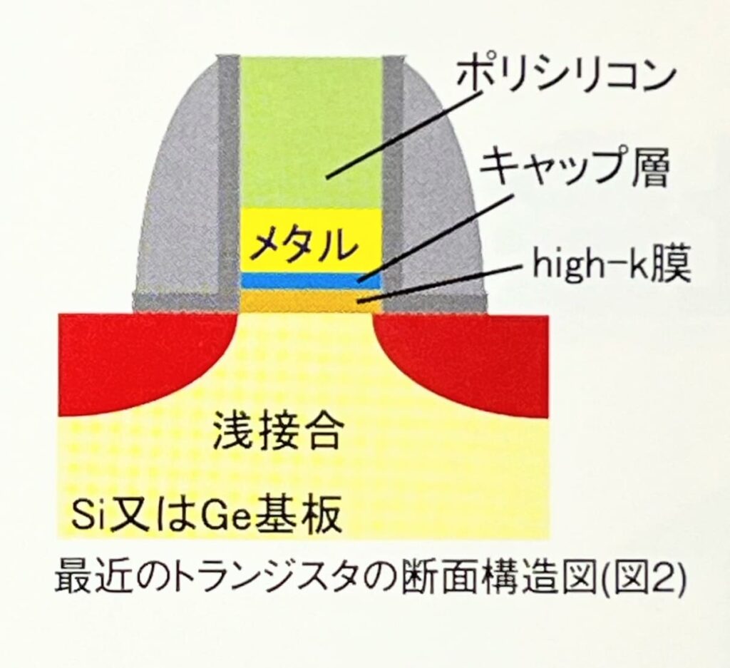
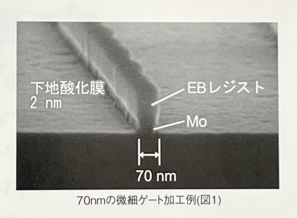
MOSFET断面写真:斜め注入Sb極浅接合によるゲートオーバーラップ調整を用いた高電流駆動力MOSFETの断面TEM写真(Top photo:XTEM photograph of high current drivability MOSFET with gate overlap length adjustment by tilt-implanted Sb ultra-shallow junctions)↩︎
【出典】K. Iwamoto, W. Mizubayashi, M. Koh, H. Murakami, T. Ono, M. Tsuno, T. Mihara, K. Shibahara, S. Yokoyama, S. Miyazaki, M. Miura-Mattausch, and M. Hirose, “Threshold voltage fluctuation induced by direct tunnel leakage current through 1.2-2.8 nm thick gate oxides for scaled MOSFETs”, Tech. Dig. International Electron Devices Meeting (IEDM 1998), pp. 923-926, 1998. [DOI: 10.1109/IEDM.1998.746504] 【関連文献】M. Koh, W. Mizubayashi, K. Iwamoto, H. Murakami, T. Ono, M. Tsuno, T. Mihara, K. Shibahara, S. Yokoyama, S. Miyazaki, M. Miura-Mattausch, and M. Hirose, “Limit of gate oxide thickness scaling in MOSFETs due to apparent threshold voltage fluctuation induced by tunnel leakage current”, Tech. Dig. International Electron Devices Meeting (IEDM 1998), pp. 919-922, 1998. [DOI: 10.1109/IEDM.1998.746503] ↩︎
【出典】M. Tsuno, M. Tanaka, M. Koh, K. Iwamoto, H. Murakami, K. Shibahara, and M. Mattausch, “Suppression of reverse-short-channel effect in sub-0.1 m n-MOSFETs with Sb S/D implantation”, Electron. Lett., Vol. 35, No. 6, pp. 508-509, 1999. 【関連文献】K. Shibahara, K. Egusa, and K. Kamesaki, “Improvement in sheet resistance of Sb-doped ultra shallow junction by dopant pileup reduction at the /Si interface”, Ext. Abstr. of the Int. Conf. on Solid State Devices and Materials (SSDM’99), pp. 514-515, 1999. [DOI: 10.7567/SSDM.1999.B-15-1] 【関連文献】K. Shibahara, “Ultra-shallow junction formation with antimony implantation”, IEICE Trans. Electron., Vol. E85-C, No. 5, pp. 1091-1097, 2002 (Invited). [DOI: 10.1587/e85-c_5_1091] ↩︎
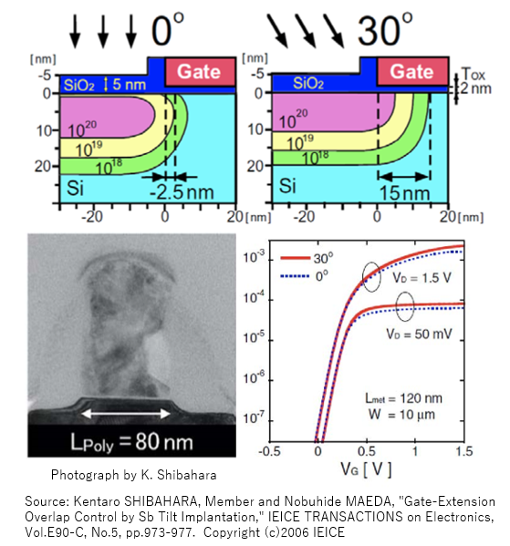
【出典】N. Maeda, D. Onimatsu, Y. Ishikawa, and K. Shibahara, “Gate-extension overlap control by Sb tilt implantation”, Proc. of the 2nd Int. Semiconductor Tech. Conf. (ISTC2002), Vol. 2002-17, pp. 165-171, 2002. 【関連文献】K. Shibahara and N. Maeda, “Gate-Extension Overlap Control by Sb Tilt Implantation”, IEICE Transactions on Electronics, Vol. E90-C, No. 5, pp. 973-977, 2007. [DOI: 10.1093/ietele/e90-c.5.973] ↩︎
【出典】M. Hino, T. Amada, N. Maeda, and K. Shibahara, “Influence of nitrogen profile on metal workfunction in Mo//Si MOS structure”, Ext. Abst. Int. Conf. on Solid State Devices and Materials (SSDM’03), pp. 494-495, 2003. 【関連文献】M. Hino, T. Amada, N. Maeda, and K. Shibahara, “Control of Mo Work Function by Solid-Phase Diffusion of Nitrogen”, Japanese Journal of Applied Physics, Vol. 45, No. 4B, pp. 2925-2928, 2006. [DOI: 10.1143/JJAP.45.2925] ↩︎
【出典】K. Sano, M. Hino, N. Ooishi, and K. Shibahara, “Workfunction tuning using various impurities for fully silicided NiSi gate”, Ext. Abst. Int. Conf. on Solid State Devices and Materials (SSDM’04), pp. 456-457, 2004. [DOI: 10.7567/SSDM.2004.p3-6] 【関連文献】K. Sano, M. Hino, and K. Shibahara, “Workfunction Tuning for Single-Metal Dual-Gate CMOS with Mo and NiSi Electrodes”, IEICE Transactions on Electronics, Vol. E88-C, No. 4, pp. 581-587, 2005. ↩︎
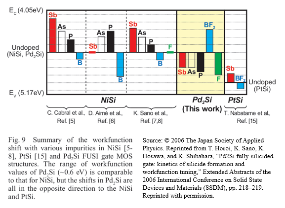
T【出典】. Hosoi, K. Sano, K. Hosawa, and K. Shibahara, “Si pd2Si fully-silicided gate: kinetics of silicide formation and workfunction tuning”, Ext. Abst. Int. Conf. on Solid State Devices and Materials (SSDM’06), pp. 218-219, 2006. [DOI: 10.7567/SSDM.2006.j-2-2] 【関連文献】T. Hosoi, K. Sano, K. Hosawa, and K. Shibahara, “Formation kinetics and workfunction tuning of Si fully silicided metal gates”, Jpn. J. Appl. Phys., Vol. 46, No. 4B, pp. 1929-1933, 2007. [DOI: 10.1143/JJAP.46.1929] ↩︎
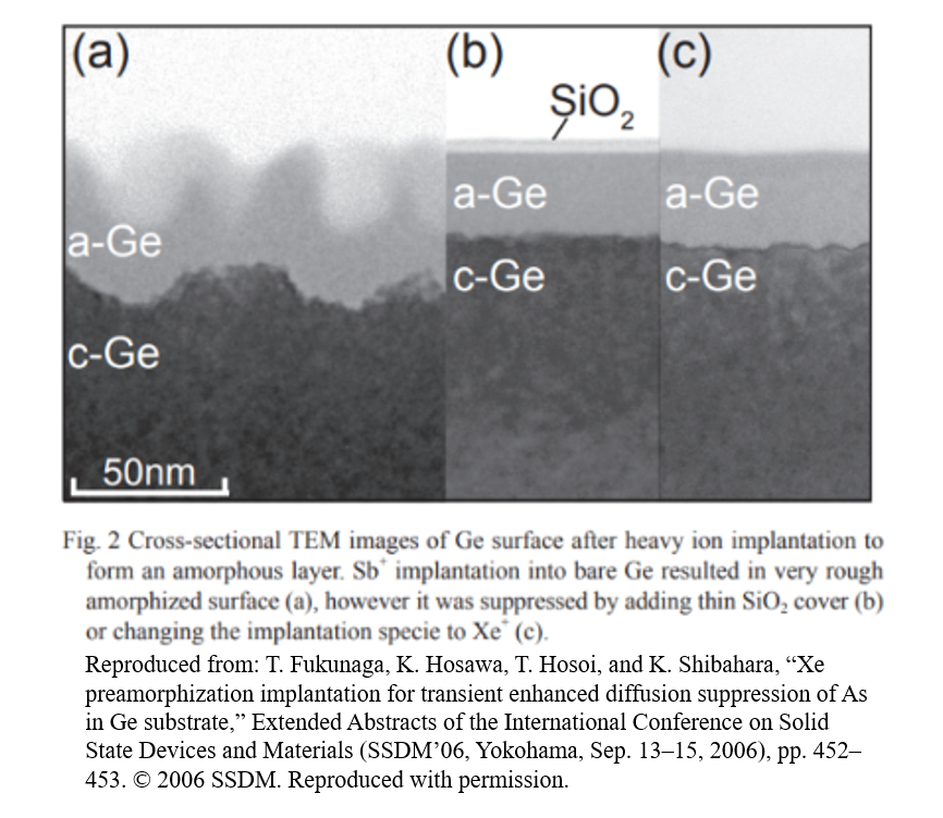
【出典】T. Fukunaga, K. Hosawa, T. Hosoi, and K. Shibahara, “Xe Preamorphization Implantation for Transient Enhanced Diffusion Suppression of As in Ge Substrate”, Extended Abstracts of the International Conference on Solid State Devices and Materials (SSDM’06), pp. 452-453, 2006. ↩︎