K. Shibahara, S. Nishino, and H. Matsunami, “Metal-oxide-semiconductor characteristics of chemical vapor-deposited cubic-SiC”, Jpn. J. Appl. Phys., 23 (1984) L862-L864.[DOI: 10.1143/JJAP.23.L862]
-1985–
S. Dohmae, K. Shibahara, S. Nishino, and H. Matsunami, “Plasma-etching of CVD grown cubic SiC single crystals”, Jpn. J. Appl. Phys., 24 (1985) L873-L875. [DOI: 10.1143/JJAP.24.L873]
-1986-
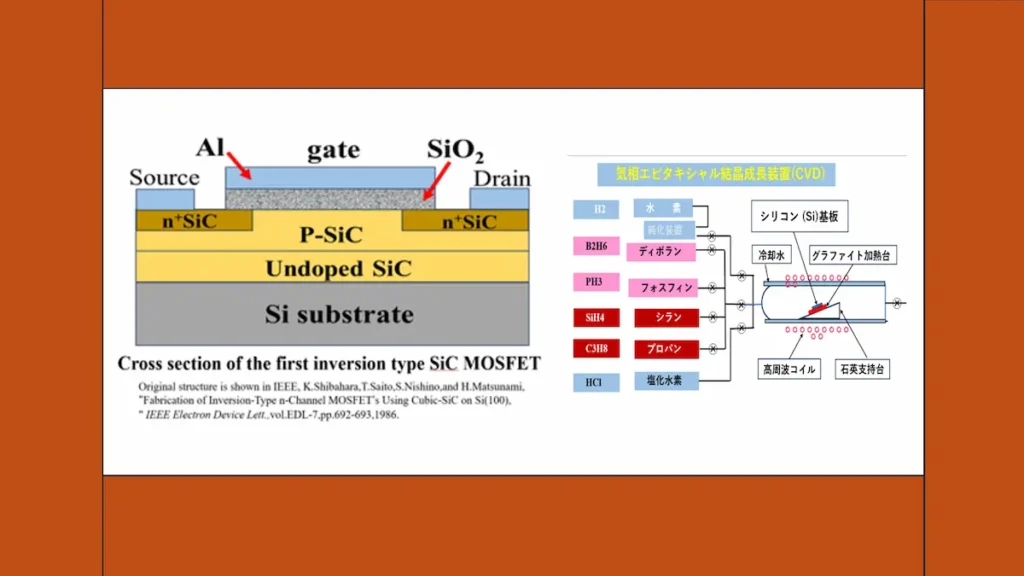
[Selected]K. Shibahara, T. Saito, S. Nishino, and H. Matsunami, “Fabrication of inversion-type n-channel MOSFETs using cubic SiC on Si(100)”, IEEE Electron Device Lett.,7 (1986) 692-693.[DOI: 10.1109/EDL.1986.26522]
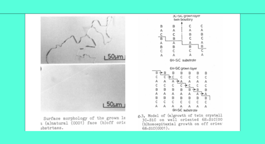
K. Shibahara, S. Nishino, and H. Matsunami, “Surface-morphology of cubic SiC(100) grown on Si(100) by chemical vapor deposition”, J. Crystal Growth 78 (1986) 538-544. [DOI: 10.1016/0022-0248(86)90158-2]
-1987-
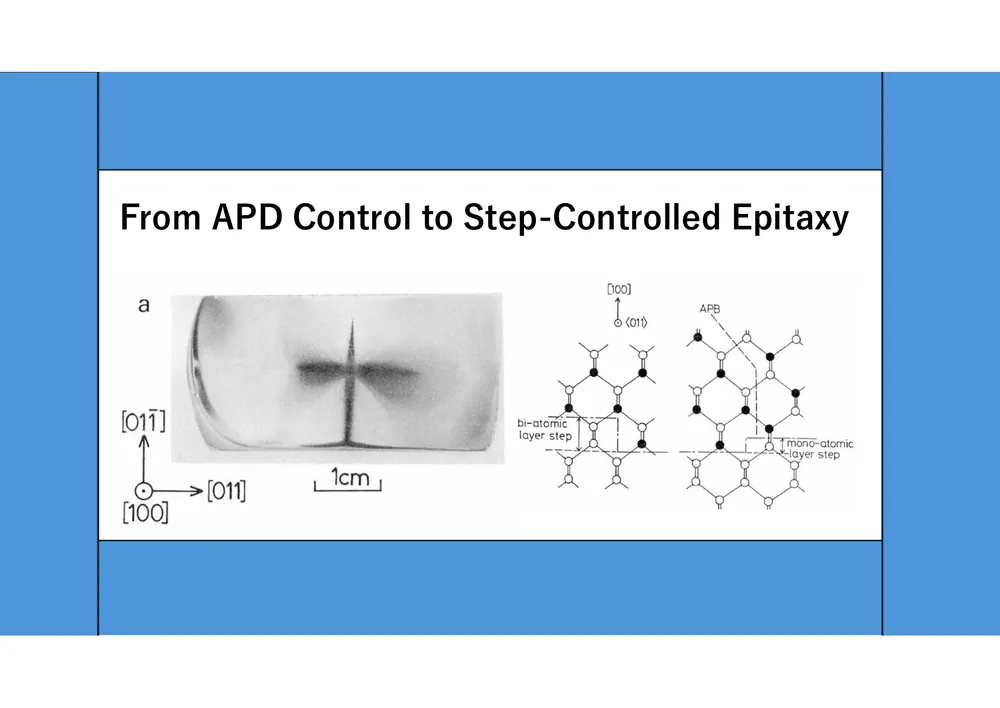
[Selected]K. Shibahara, S. Nishino, and H. Matsunami, “Antiphase-domain-free growth of cubic SiC on Si(100)”, Appl. Phys. Lett., 50 (1987) 1888-1890. [DOI: 10.1063/1.97676]
K. Shibahara, N. Kuroda, S. Nishino, and H. Matsunami, “Fabrication of p-n-junction diodes using homoepitaxially grown 6H-SiC at low temperature by chemical vapor-deposition”, Jpn. J. Appl. Phys., 26 (1987) L1815-L1817. [DOI:10.1143/JJAP.26.L1815]
-1988-
M. Iwami, M. Kusaka, M. Hirai, H. Nakamura, K. Shibahara, and H. Matsunami, “A New application of soft-X-ray spectroscopy to a non-destructive analysis of a film substrate contact system – Carbonized-layer (ultra-thin-film) Si(100)”, Surf. Sci., 199 (1988) 467-475. [DOI:10.1016/0039-6028(88)90915-6]
M. Iwami, M. Kusaka, M. Hirai, H. Nakamura, T. Koshikawa, K. Shibahara, and H. Matsunami, “Compositional analysis of semiconductor heterojunctions – Structure of SiC (thin buffer layer)/SI(100) system”, Nucl. Instr. and Meth. B, 33 (1988) 615-618. [DOI:10.1016/0168-583X(88)90643-X]
1989-1995
-1989-
K. Shibahara, T. Takeuchi, S. Nishino, and H. Matsunami, “Electrical–properties of undoped and ion-implanted cubic SiC grown on Si(100) by chemical vapor-deposition”, Jpn. J. Appl. Phys., 28 (1989) 1341-1347. [DOI: 10.1143/jjap.28.1341]
H. Hida, Y. Tsukada, Y. Ogawa, H. Toyoshima, M. Fujii, K. Shibahara, M. Kohno, and T. Nozaki, “High-speed and large noise margin tolerance E/D logic gates with LDD structure DMTs fabricated using selective RIE technology”, IEEE Trans. Electron Devices,36 (1989) 2223-2230. [DOI:10.1109/16.40903]
-1992-
A. Tanabe, T. Takeshima, H. Koike, Y. Aimoto, M. Takeda, T. Ishijima, N. Kasai, H. Hada, K. Shibahara, T. Kunio, T. Tanigawa, T. Saeki, M. Sakao, H. Miyamoto, H. Nozue, S. Ohya, T.Murotani, K. Koyama, and T. Okuda, “A 30-ns 64-Mb DRAM with built-in self-test and self-repair function”, IEEE J. Solid-State Circuits, 27 (1992) 1525-1533. [DOI:10.1109/4.165332]
-1993-
T. Sugibayashi, T. Takeshima, I. Naritake, T. Matano, H. Takada, Y. Aimoto, K. Furuta, M. Fujita, T. Saeki, H. Sugawara, T. Murotani, N. Kasai, K. Nakajima, H. Hada, T. Hamada, N. Aizaki, T. Kunio, E. Kakehashi, K. Masumori, K. Shibahara, and T. Tanigawa, “A 30-ns 256-Mb DRAM with a multidivided array structure”, IEEE J. Solid-State Circuits, 28 (1993) 1092-1098. [DOI: 10.1109/4.245587]
-1995- T. Sugibayashi, I. Naritake, S. Utsugi, K. Shibahara, R. Oikawa, H. Mori, S. Iwao, T. Murotani, K. Koyama, S. Fukuzawa, T. Itani, K. Kasama, T. Okuda, S. Ohya, and M. Ogawa, “A 1-Gb DRAM for file applications”, IEEE J. Solid-State Circuits, 30 (1995) 1277-1280. [DOI: 10.1109/4.475717]
1996-2012(広島大学)
-1996-
T. Doi, T. Namba, A. Uehara, M. Nagata, S. Miyazaki, K. Shibahara, S. Yokoyama, A. Iwata, T. Ae, and M. Hirose, “Optically interconnected Kohonen net for pattern recognition”, Jpn. J. Appl. Phys., 35 (1996) 1405-1409. [DOI:10.1143/JJAP.35.1405]
T. Namba, A. Uehara, T. Doi, T. Nagata, Y. Kuroda, S. Miyazaki, K. Shibahara, S. Yokoyama, A. Iwata, and M. Hirose, “High-efficiency micromirrors and branched optical waveguides on Si chips”, Jpn. J. Appl. Phys., 35 (1996) 941-945. [DOI:10.1143/JJAP.35.941]
H. Goto, K. Shibahara, and S. Yokoyama, “Atomic layer controlled deposition of silicon nitride with self-limiting mechanism”, Appl. Phys. Lett., 68 (1996) 3257-3259. [DOI:10.1063/1.116566]
-1997-
S. Yokoyama, H. Goto, T. Miyamoto, N. Ikeda, and K. Shibahara, “Atomic layer controlled deposition of silicon nitride and in situ growth observation by infrared reflection absorption spectroscopy”, Appl. Surf. Sci., 112 (1997) 75-81.[DOI:10.1016/s0169-4332(96)01020-3]
J. Maeda, Y. Sasaki, N. Dietz, K. Shibahara, S. Yokoyama, S. Miyazaki, and M. Hirose, “High-rate GaAs epitaxial lift-off technique for optoelectronic integrated circuits”, Jpn. J. Appl. Phys., 36 (1997) 1554-1557. [DOI:10.1143/JJAP.36.1554]
-1998-
H. Tobimatsu, Y. Inoue, T. Seto, K. Okuyama, T. Fujii, K. Shibahara, S. Yokoyama, and M. Hirose, “Reduction of gaseous contamination by UV/photoelectron method”, IEEE Trans. Semicond. Manufact., 11 (1998) 9-12. [DOI: 10.1109/66.661281]
M. Tsuno, S. Yokoyama, and K. Shibahara, “A Study of electrical characteristics improvements in sub-0.1 μm gate length MOSFETs by low temperature operation”,IEICE Trans. Electron. E81-C (1998), 1913-1917. [DOI: 10.1587/e81-c_12_1913]
M. Tsuno, S. Yokoyama and K. Shibahara, “New Ar-plasma cleaning process for reduction of Al/TiSi2 contact resistance”, Jpn. J. Appl. Phys., 37 (1998) 5902-5905. [DOI:10.1143/JJAP.37.5902]
-1999-
M. Tsuno, M. Tanaka, M. Koh, K. Iwamoto, H. Murakami, K. Shibahara, and M. Mattausch, “Suppression of reverse-short-channel effect in sub-0.1 μm n-MOSFETs with Sb S/D implantation”, Electron. Lett., 35 (1999) 508-509. [DOI:10.1049/el:19990325]
M. Koh, K. Egusa, H. Furumoto, T. Shirakata, E. Seo, K. Shibahara, S. Yokoyama, and M. Hirose, “Quantitative evaluation of dopant loss in 5-10 keV As ion implantation for low-resistive, ultrashallow source/drain formation”, Jpn. J. Appl. Phys., 38 (1999) 2324-2328. [DOI:10.1143/JJAP.38.2324]
Y. Sasaki, T. Katayama, T. Koishi, K. Shibahara, S. Yokoyama, S. Miyazaki, and M. Hirose, “High-speed GaAs epitaxial lift-off and bonding with high alignment accuracy using a sapphire plate”, J. Electrochem. Soc., 146 (1999) 710-712.[DOI:10.1149/1.1391668]
T. Hatano, A. Nomura, M. Yoshida, A. Nakajima, K. Shibahara, and S. Yokoyama, “Calculation of electrical properties of novel double-barrier metal oxide semiconductor transistors”, Jpn. J. Appl. Phys., 38 (1999) 399-402. [DOI:10.1143/JJAP.38.399]
M. Tsuno, M. Suga, M. Tanaka, K. Shibahara, M. Miura-Mattausch, and M. Hirose, “Physically-based threshold voltage determination for MOSFET’s of all gate lengths”, IEEE Trans. Electron Devices, 46 (1999) 1381–1387. [DOI:10.1109/16.772487]
Y. Aoki, N. Kawakami, K. Shibahara, S. Yokoyama, “Evaluation of stress induced defects due to recessed LOCOS process”, J. Korean Phys., Soc. 35. Suppl. (1999), pp. S76-S79.
-2000-
K. Shibahara, K. Egusa, K. Kamesaki, and H. Furumoto, “Improvement in antimony-doped ultra shallow junction sheet resistance by dopant pileup reduction at the SiO2 /Si interface”, Jpn. J. Appl. Phys., 39 (2000) 2194-2197. [DOI:10.1143/JJAP.39.2194]
M. Hirose, M. Koh, W. Mizubayashi, H. Murakami, K. Shibahara, and S. Miyazaki, “Fundamental limit of gate oxide thickness scaling in advanced MOSFETs”, Semiconductor Sci. & Technol. 15 (2000) 485-490. [DOI:10.1088/0268-1242/15/5/308]
M. Hirose, W. Mizubayashi, Khairurrijal, M. Ikeda, H. Murakami, A. Kohno, K. Shibahara, and S. Miyazaki, “Ultrathin gate dielectrics for silicon nanodevices”, Superlattices & Microstructures, 27 (2000) 383-393. [DOI: 10.1006/spmi.2000.0861]
-2001-
[Selected] M. Koh, W. Mizubayashi, K. Iwamoto, H. Murakami, T. Ono, M. Tsuno, T. Mihara, K. Shibahara, S. Miyazaki, and M. Hirose, “Limit of gate oxide thickness scaling in MOSFETs due to apparent threshold voltage fluctuation induced by tunnel leakage current”, IEEE Trans. Electron Devices, 48 (2001) 259-264. [DOI:10.1109/16.902724]
D. Notsu, N. Ikeuchi, Y. Aoki, N. Kawakami, and K. Shibahara, “Fabrication of 100 nm width fine active-region using LOCOS isolation”, IEICE Trans. Electronics, E85-C (2002) 1119-1123. [DOI:10.1587/e85-c_5_1119]
K. Shibahara, D. Onimatsu, Y. Ishikawa, T. Oda, and T. Kikkawa, “Copper drift in low dielectric constant insulator films caused by O2+ primary ion beam”, Appl. Surf. Sci., 203-204 (2002) 387-390. [DOI:10.1016/S0169-4332(02)00682-7]
-2003-
K. Imai, S. Shishiguchi, K. Shibahara and S. Yokoyama, “Phosphorus-assisted low-energy arsenic implantation technology for n-channel metal-oxide-semiconductor field-effect transistor source/drain formation process”, Jpn. J. Appl. Phys., 42 (2003) 2654-2659.[DOI:10.1143/JJAP.42.2654]
S. Nakamura, M. Itano, H. Aoyama, K. Shibahara, S. Yokoyama and M. Hirose, “Comparative studies of perfluorocarbon alternative gas plasmas for contact hole etch”, Jpn. J. Appl. Phys., 42 (2003) 5759-5764. [DOI:10.1143/jjap.42.5759]
Q. Khosru, S. Yokoyama, A. Nakajima, K. Shibahara, T. Kikkawa, H. Sunami, and T. Yoshino, “Organic contamination dependence of process-induced interface trap generation in ultrathin oxide metal oxide semiconductor transistors”, Jpn. J. Appl. Phys., 42 (2003) L1429-L1432. [DOI:10.1143/jjap.42.l1429]
-2005-
A. Matsuno, E. Takii, T. Eto, K. Kurobe, and K. Shibahara, “Merits and demerits of light absorbers for ultra shallow junction formation by green laser annealing”, Nucl. Instr. and Meth. B, 237 (2005) 136-141. [DOI: 10.1016/j.nimb.2005.04.088]
K. Kobayashi, T. Eto, K. Okuyama, K. Shibahara, and H. Sunami, “Application of Arsenic Plasma Doping in Three-Dimensional MOS Transistors and the Doping Profile Evaluation”, Jpn. J. Appl. Phys., 44 (2005) 2273-2278. [DOI: 10.1143/JJAP.44.2273]
T. Eto and K. Shibahara, “Accuracy of SIMS depth profiling for sub-keV As+ implantation”, Jpn. J. Appl. Phys., 44 (2005) 2433-2436. [DOI: 10.1143/JJAP.44.2433]
E. Takii, T. Eto, K. Kurobe, and K. Shibahara, “Ultra shallow junction formation by green-laser annealing with light absorber”, Jpn. J. Appl. Phys., 44 (2005) L756-L759. [DOI: 10.1143/JJAP.44.L756]
[Selected] K. Sano, M. Hino, N. Ooishi, and K. Shibahara, “Workfunction tuning using various impurities for fully silicided NiSi”, Jpn. J. Appl. Phys., 44 (2005) 3774-3777. [DOI: 10.1143/JJAP.44.3774]
T. Tanaka, S. Watanabe, K. Shibahara, S. Yokoyama and T. Takagi, “Plasma-based ion implantation sterilization technique and ion energy estimation”, J. Vac. Sci. Technol. A, 23 (2005) 1018-1021. [DOI: 10.1116/1.1943468]
K. Kurobe, Y. Ishikawa and K. Shibahara, “Sheet resistance reduction and crystallinity improvement in ultrashallow n+/p junctions by heat-assisted excimer laser annealing”, Jpn. J. Appl. Phys., 44 (2005) 8391-8395. [DOI:10.1143/JJAP.44.8391]
-2006-
[Selected]K. Shibahara, T. Eto, and K. Kurobe, “Merits of heat-assist for melt laser annealing”, IEEE Trans. Electron Devices, 53 (2006) 1059-1064. [DOI:10.1109/TED.2006.871870]
A. Matsuno and K. Shibahara, “Effect of Pulse Duration on Formation of Ultrashallow Junction by Excimer Laser Annealing”, Jpn. J. Appl. Phys., 45 (2006) 8537-8541. [DOI: 10.1143/JJAP.45.8537]
-2007-
T. Hosoi, K. Sano, K. Hosawa, and K. Shibahara, “Formation kinetics and workfunction tuning of Pd2Si fully silicided metal gates”, Jpn. J. Appl. Phys., 46 (2007) 1929-1933.[DOI:10.1143/JJAP.46.1929]
K. Shibahara, and N. Maeda, “Gate-extension overlap control by Sb tilt implantation”, IEICE Trans. Electron., E90-C (2007) 973-977. [DOI:10.1093/ietele/e90-c.5.973]
-2008-
T. Yamashita, Y. Nishida, T. Okagaki, Y. Miyagawa, J. Yugami, H. Oda, Y. Inoue, and K. Shibahara, “ Stress from discontinuous SiN liner for fully silicided gate process”, Jpn. J. Appl. Phys., 47 (2008) 2569-2574. [DOI:10.1143/JJAP.47.2569]
T. Hosoi, K. Sano, A. Ohta, K. Makihara, H. Kaku, S. Miyazaki, and K. Shibahara, “ Interface properties and effective work function of Sb-predoped fully silicided NiSi gate”, Surf. Interface Anal., 40 (2008) 1126-1130. [DOI:10.1002/sia.2827]
T. Yamashita, Y. Nishida, K. Eikyu, H. Oda, Y. Inoue, and K. Shibahara, “ Threshold Voltage Modulation Using N 2 + Implantation Into Substrate for Ni Fully Silicided Gate/High-k NMOS ”, IEEE Electron Device Lett., 29 (2008) 1163-1166. [DOI:10.1109/LED.2008.2004416]
-2009-
T. Hosoi, A. Ohta, S. Miyazaki, H. Shiraishi, and K. Shibahara, “Photoemission study of fully silicided Pd2Si gates with interface modification induced by dopants”, Appl. Phys. Lett., 94 (2009) 192102 (3 pages).[DOI:10.1063/1.3133337]
-2010-
M. Terai, T. Hase, K. Shibahara, H. Watanabe, “Effects of Si/Ni composition ratio of NixSiy gate electrode and Hf/Si composition ratio of Hf-based high-k insulator on threshold voltage controllability and mobility of metal-oxide-semiconductor field-effect transistors”, Jpn. J. Appl. Phys., 49 (2010) 036504 (7 pages). [DOI:10.1143/JJAP.49.036504]
Y. Nishida, K. Eikyu, A.Shimizu, T. Yamashita, H. Oda, Y. Inoue, and K. Shibahara, “Temperature coefficient of threshold voltage in high-k metal gate transistors with various TiN and capping layer thicknesses”, Jpn. J. Appl. Phys., 49 (2010) 04DC03 (5 pages). [DOI:10.1143/JJAP.49.04DC03]
-2012-
Y. Kawasaki and K. Shibahara, “Effects of B18Hx+ and B18Hx dimer ion implantations on crystallinity and retained B dose in silicon”, J. Vac. Sci. Technol. A, 30 (2012) 011601 (5 pages). [DOI:10.1116/1.3655892]
S. Nishino, K. Shibahara, S. Dohmae and H. Matsunami, “Production of Single Crystalline Cubic-SiC with 2-inch Diameter by CVD and Characteristics of MOS Diodes”, Late News Abstracts of the 16th International Conference on Solid State Devices and Materials (SSDM 1984), Kobe, pp. 8–9, 1984. [DOI: 10.7567/SSDM.1984.LD-1-4]
-1986-
K. Shibahara, T. Saito, S. Nishino, and H. Matsunami, “Inversion-type N-channel MOSFET Using Antiphase-domain Free Cubic-SiC Grown on Si(100)”, Extended Abstracts of the 18th International Conference on Solid State Devices and Materials (SSDM 1986), Tokyo, pp. 717–718, 1986.
-1987-
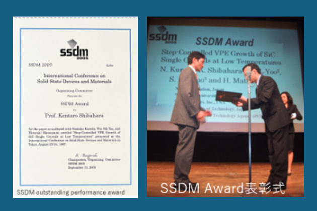
[Selected]N. Kuroda, K. Shibahara, W. Yoo, S. Nishino, and H. Matsunami, “Step-Controlled VPE Growth of SiC Single Crystals at Low Temperatures”, Ext. Abst. 19th Conf. Solid State Devices and Materials (SSDM 1987), pp. 227-230. (SSDM Award)https://doi.org/10.7567/SSDM.1987.C-4-2Full text
K. Shibahara, S. Nishino and H. Matsunami, “Heteroepitaxial growth of antiphase-boundary-free cubic SiC(100) single crystals on Si(100)”, Proc. Mat. Res. Soc., 97 (1987) 183–188. [DOI:10.1557/PROC-97-183]
K. Shibahara, T. Takeuchi, T. Saitoh, S. Nishino and H. Matsunami, “Inversion-type MOS field effect transistors using CVD grown cubic SiC on Si”, Proc. Mat. Res. Soc., 97 (1987) 247-252. [DOI: 10.1557/proc-97-247]
1988-1995 (NEC)
-1988-
H. Hida, Y. Tsukada, Y. Ogawa, H. Toyoshima, M. Fujii, K. Shibahara, M. Kohno, T. Nozaki, “Novel self-aligned gate process technology for i-AlGaAs/n-GaAs doped-channel hetero-MISFET(DMT) LSIs based on E/D logic gates,” Technical Digest. International Electron Devices Meeting (IEDM), 1988, pp. 688-691, [DOI:10.1109/IEDM.1988.32906]
-1989-
M. Fujii, H. Hida, Y. Tsukada, Y. Ogawa, M. Kohno, K. Shibahara, H. Toyoshima, K. Shimizu, T. Misaki, “High speed and low power consumption DMT integrated circuits based on direct-coupled FET logic circuits,” Technical Digest. International Electron Devices Meeting (IEDM), 1989, pp. 113-116, [DOI:10.1109/IEDM.1989.74240]
H. Matsunami, K. Shibahara, N. Kuroda, W. Yoo, and S. Nishino, “VPE Growth of SiC on Step-Controlled Substrates,” in Amorphous and Crystalline Silicon Carbide and Related Materials, Springer Proceedings in Physics, Vol. 34 (1989), pp. 34–39. [DOI: 10.1007/978-3-642-93406-3_3]
-1990-
K. Shibahara, Y. Ogawa, H. Toyoshima, H. Hida, T. Maeda, and K. Ohata, “Low-temperature buffer introduction into self-aligned refractory-metal gate DMTs”, IOP Conf. Ser., 112 (1990) 257-262.
-1992-
[Selected]K. Shibahara, Y. Fujimoto, M. Hamada, S. Iwao, K. Tokashiki, and T. Kunio, “Trench isolation with ∇-shaped buried oxide for 256 Mega-bit DRAMs”, 1992 International Electron Devices Meeting (IEDM), pp. 275-278, 1992. [DOI: 10.1109/IEDM.1992.307359 ]
H. Koike, A. Tanabe, T. Takeshima, Y. Aimoto, M. Takada, T. Ishijima, N. Kasai, H. Hada, K. Shibahara, T. Kunio, T. Tanigawa, T. Saeki, M. Sakao, H. Miyamoto, H. Nozue, S. Ohya, T. Murotani, K. Koyama, and T. Okuda, “A 30-ns 64-Mb DRAM with built-in self-test and repair function”, Digest of Technical Papers, 1992 IEEE International Solid-State Circuits Conference (ISSCC 1992), pp. 150-151, 1992. [DOI:10.1109/ISSCC.1992.200456] .
-1994-
[Selected]K. Shibahara, H. Mori, S. Ohnishi, R. Oikawa, K. Nakajima, Y. Kojima, H. Yamashita, K. Itoh, S. Kamiyama, H. Watanabe, T. Hamada, and K. Koyama, “1G DRAM cell with diagonal bit-line (DBL) configuration and edge operation MOS (EOS) FET”, Tech. Dig. 1994 International Electron Devices Meeting (IEDM 1994), pp. 639–642. [DOI:10.1109/IEDM.1994.383329]
P.-Y. Lesaicherre, S. Yamamichi, H. Yamaguchi, K. Takemura, H. Watanabe, K. Tokashiki, K. Satoh, T. Sakuma, M. Yoshida, S. Ohnishi, K. Nakajima, K. Shibahara, Y. Miyasaka, and H. Ono, “A Gbit-scale DRAM stacked capacitor technology with ECR MOCVD SrTiO3 and RIE patterned RuO2/TiN storage nodes”, Technical Digest of International Electron Devices Meeting (IEDM 1994), pp. 731-733. [DOI:10.1109/IEDM.1994.383296]
1995-2000(広島大学)
-1995-
T. Sugibayashi, I. Naritake, S. Utsugi, K. Shibahara, R. Oikawa, H. Mori, S. Iwao, T. Murotani, K. Koyama, S. Fukuzawa, T. Itani, K. Kasama, T. Okuda, S. Ohya, and M. Ogawa, “A 1Gb DRAM for File Applications”, IEEE International Solid-State Circuits Conference (ISSCC 1995), Digest of Technical Papers, pp. 254-255, 1995. .
T. Namba, A. Uehara, T. Doi, T. Nagata, Y. Kuroda, S. Miyazaki, K. Shibahara, S. Yokoyama, A. Iwata and M. Hirose, “High-Efficiency Micromirrors and Branched Optical Waveguides on Si Chips”, Extended Abstracts of the 1995 International Conference on Solid State Devices and Materials (SSDM 1995, Osaka, Japan, August 21–24, 1995), C-5-2, pp. 830–832. [DOI: 10.7567/SSDM.1995.C-5-2].
T. Doi, T. Namba, A. Uehara, M. Nagata, S. Miyazaki, K. Shibahara, S. Yokoyama, A. Iwata, T. Ae and M. Hirose, “Optically Interconnected Kohonen Net for Pattern Recognition”, Extended Abstracts of the 1995 International Conference on Solid State Devices and Materials (SSDM 1995, Osaka, Japan, August 21–24, 1995), LB-L7, pp. 1075–1076..
-1996-
[Selected]K. Shibahara, N. Mifuji, K. Kawabata, T. Kugimiya, H. Furumoto, M. Tsuno, S. Yokoyama, M. Nagata, S. Miyazaki, and M. Hirose, “Low Resistive Ultra Shallow Junction for Sub 0.1μm MOSFETs Formed by Sb Implantation”, International Electron Devices Meeting (IEDM) , San Francisco 1996., pp.579 – 582. [DOI:10.1109/IEDM.1996.554050]
J. Maeda, Y. Sasaki, K. Shibahara, S. Yokoyama, S. Miyazaki, and M. Hirose, “High-Rate GaAs Epitaxial Lift-Off Technique for Optoelectronic Integrated Circuits”, Ext. Abst. 28th Conf. Solid State Devices and Materials (SSDM 1996), pp. 383-385. [DOI:10.7567/SSDM.1996.D-4-3]
-1997-
K. Shibahara, S. Yokoyama, H. Tobimatsu, W. Mizubayashi, M. Hirose, and T. Fujii, “ Reliability evaluation of ultrathin gate oxides grown on Si wafers stored in clean stocker with a UV/photoelectron source”, Proc. 1997 IEEE Int. Symp. on Semiconductor Manufacturing (ISSM 1997), (San Francisco, Oct. 6-8) pp. F5-F8. [DOI:10.1109/ISSM.1997.664596]
-1998-
M. Koh, K. Iwamoto, W. Mizubayashi, H. Murakami, T. Ono, M. Tsuno, T. Mihara, K. Shibahara, S. Yokoyama, S. Miyazaki, M. Miura-Mattausch, and M. Hirose, “Threshold voltage fluctuation induced by direct tunnel leakage current through 1.2-2.8 nm thick gate oxides for scaled MOSFETs”, Tech. Dig. International Electron Devices Meeting (IEDM 1998), pp. 919-922, 1998. [DOI: 10.1109/IEDM.1998.746504]
M. Koh, K. Egusa, H. Furumoto, K. Shibahara, S. Yokoyama and M. Hirose, “Quantitative evaluation of dopant loss in low energy As implantation for low-resistive, ultra shallow source/drain formation”, Extend. Abst. of the Int. Conf. on Solid State Devices and Materials (SSDM’98), pp. 18-19. [DOI: 10.7567/SSDM.1998.A-1-6]
K. Shibahara, H. Furumoto, K. Egusa, M. Koh and S. Yokoyama, “Dopant loss origins of low energy implanted arsenic and antimony for ultra shallow junction formation”, Mat. Res. Soc. Symp. Proc., 532 (1998), pp. 23-28. [DOI:10.1557/proc-532-23]
K. Egusa and K. Shibahara, “Influence of high dose low energy ion implantation on dopant depth profile”, Proceedings of the 1998 International Conference on Ion Implantation Technology (IIT ’98), 2, 1998, pp. 724-727. [DOI:10.1109/IIT.1998.813769]
M. Tsuno, K. Shibahara, M. Miura-Mattausch, M. Hirose, M. Suga, and M. Tanaka, “Reliable threshold voltage determination for sub-0.1 μm gate length MOSFETs”, Proceedings of 1998 Asia and South Pacific Design Automation Conference (ASP-DAC ’98), (1998) pp. 111-116.
-1999-
K. Shibahara, K. Kamesaki, and K. iEgusa, “Improvement in sheet resistance of Sb-doped ultra shallow junction by dopant pileup reduction at the SiO2/Si interface”, Extend. Abst. of the Int. Conf. on Solid State Devices and Materials (SSDM’99), pp. 514-515. [DOI:10.7567/SSDM.1999.B-15-1]
-2001-
K. Shibahara, “Doping issues for sub-100 nm MOSFETs”, Proc. of 2001 Korea-Japan Joint Workshop on Advanced Semiconductor Processes and Equipments (ASPE2001), pp. 160-164, 2001.
D. Onimatsu and K. Shibahara, “Influence of extension formation process of indium halo profile”, Extend. Abst. of the Int. Conf. on Solid State Devices and Materials (SSDM2001), pp. 184-185, 2001 [DOI:10.7567/SSDM.2001.A-5-4]
K. Shibahara, Y. Ishikawa, D. Onimatsu, N. Maeda, A. Mineji, K. Kagawa, A. Matuno, and T. Nire, “Antimony behavior in laser annealing process for ultra shallow junction formation”, Extend. Abst. of the Int. Conf. on Solid State Devices and Materials (SSDM2001), pp. 236-237, 2001 [DOI:10.7567/SSDM.2001.LB-2-2]
K. Shibahara, T. Oda, and T. Kikkawa, “Copper drift in low dielectric constant insulator films caused by O2+ primary ion beam”, Abst. 13th Int. Conf. on Secondary Ion Mass Spectrometry and Related Topics (SIMSXIII), p. 37, 2001.
N. Kawakami, K. Egusa, and K. Shibahara, “Reduction of threshold voltage fluctuation of p-MOSFETs by antimony super steep retrograde well channel”, Extended Abstracts of the Second International Workshop on Junction Technology (IWJT 2001), 2001. [DOI:10.1109/IWJT.2001.993814] .
-2002-
T. Amada, N. Maeda, and K. Shibahara, “Degradation in a molybdenum-gate MOS structure caused by N+ ion implantation for work function control”, Mat. Res. Soc. Symp. Proc. 716 (2002) 299-314. [DOI:10.1557/PROC-716-B7.5]
N. Maeda, D. Onimatsu, Y. Ishikawa and K. Shibahara, “Gate-extension overlap control by Sb tilt implantation”, Proc. of the 2nd Int. Semiconductor Tech. Conf. (ISTC2002), 2002-17, pp. 165-171, 2002.
A. Matsuno, K. Kagawa, Y. Niwatsukino, T. Nire, and K. Shibahara, “Pulse duration effects on laser anneal shallow junction”, Proc. of the 2nd Int. Semiconductor Tech. Conf. (ISTC2002), Vol.2002-17, pp. 148-156, 2002.
K. Kurobe, Y. Ishikawa, K. Kagawa, Y. Niwatsukino, A. Matsuno, and K. Shibahara, “Formation of low-resistive ultra-shallow n+/p junction by heat-assisted excimer laser annealing”, Int. Workshop on Junction Tech. (IWJT’02), pp. 35-36, 2002. [DOI: 10.1109/IWJT.2002.1225194]
-2003-
K. Shibahara, K. Kurobe, Y. Ishikawa, K. Kagawa, Y. Niwatsukino, and A. Matsuno, “KRF excimer laser annealing for ultra shallow junction formation: approach for irradiation energy density reduction”, Extend. Abst. 11th Int. Conf. on Adv. Thermal Processing of Semiconductors (RTP 2003), pp. 13-16, 2003. [Invited]. [DOI: 10.1109/RTP.2003.1249119]
K. Kurobe, Y. Ishikawa, K. Kagawa, Y. Niwatsukino, A. Matsuno, and K. Shibahara, “Defect density reduction and sheet resistance improvement by multi-pulse KrF-excimer-laser annealing”, Extend. Abst. Fabrication, Characterization, and Modeling of Ultra-Shallow Doping Profiles in Semiconductors (USJ 2003), pp. 98-103, 2003.
K. Imai, S. Maruyama, T. Suzuki, T. Kudo, S. Miyake, M. Ikeda, T. Abe, S. Masuda, A. Tanabe, J.-W. Lee, K. Shibahara, S. Yokoyama and H. Ooka, “60-nm gate length SOI CMOS technology optimized for system-on-a-SOI-chip solution”, Proc. of the 203rd Meeting of Electrochemical Society, Silicon-on-insulator Technology and Devices XI, pp. 149-158, (2003).
M. Hino, T. Amada, N. Maeda, and K. Shibahara, “Influence of nitrogen profile on metal workfunction in Mo/SiO2/Si MOS structure”, Ext. Abst. Int. Conf. on Solid State Devices and Materials (SSDM’03), pp. 494-495, 2003.
M. Murakawa, K. Shibahara, Y. Oda, T. Higuchi, and K. Nishi, “Ultra-shallow boron profile fitting compensating for surface contamination by utilizing genetic algorithms”, Ext. Abst. Int. Conf. on Solid State Devices and Materials (SSDM’03), pp. 504-505, 2003. [DOI: 10.7567/SSDM.2003.P4-7]
-2004-
Masahiko Shibahara, Susumu Kotake, Takayoshi Inoue, Akira Matsuno, Kazuhiro Kagawa, and K. Shibahara, “Molecular dynamics simulation on excimer laser annealing process for ultra shallow junction formation”, The 1st Int. Symp. on Micro & Nano Technology, pp. VIII-1-02-1-VIII-1-02-5, 2004.
T. Eto, and K. Shibahara, “Precise Depth Profiling of Sub-keV Implantated Arsenic”, Ext. Abst. 2004 Int. Conf. on Solid State Devices and Materials (SSDM’04), pp. P5-11, 2004. [DOI: 10.7567/SSDM.2004.P5-11]
K. Sano, M. Hino, N. Ooishi, and K. Shibahara, “Workfunction tuning using various impurities for fully silicided NiSi gate”, Ext. Abst. Int. Conf. on Solid State Devices and Materials (SSDM’04), pp. 456-457, [DOI:10.7567/SSDM.2004.P3-6]
K. Sano, M. Hino, and K. Shibahara, “Workfunction Tuning for Single-Metal Dual-Gate CMOS with Mo and NiSi Electrodes”, Ext. Abst. 2004 Int. Conf. on Solid State Devices and Materials (SSDM’04), pp. 454-455, 2004. [DOI: 10.7567/SSDM.2004.F-2-8]
E. Takii, T. Eto, K. Kurobe, A. Matsuno, and K. Shibahara, “Merits and demerits of light absorber for ultra shallow junction formation by green laser annealing”, Int. Conf. on Ion Implantation Technology (IIT’04), p. 63, 2004.
K. Shibahara, K. Kurobe and T. Eto, “Sub-20-nm junction formation by heat-assisted laser annealing”, Proceedings of 2004 Korea-Japan Joint Workshop on Advanced Semiconductor Processes and Equipments (ASPE 2004), pp. 162-165.
-2005-
K. Shibahara, “Benefits of heat-assist for laser annealing”, Ext. Abst. of Int. Workshop on Junction Technology, (IWJT’05, Osaka, Jun. 6-7, 2005), pp. 53-54,(Invited). [DOI: 10.1109/IWJT.2005.203880]
T. Hosoi, M. Hino, K. Sano, N. Ooishi, and K. Shibahara, “Molybdenum-gate MOSFET threshold voltage modification based on two-dimensional nitrogen distribution control in gate electrode”, Abstracts of MRS 2005 spring meeting, pp.191-192.
K. Hosawa, K. Matsumoto, and K. Shibahara, “Anomalous doping profile in heavily doped Ge”, Extended Abstracts of Int. Workshop on Junction Technology, (IWJT’05 ,Osaka, Jun. 6-7, 2005), pp. 39-40.[DOI: 10.1109/IWJT.2005.203875]
A. Matsuno, and K. Shibahara, “Function of phase switch layer for ultra shallow junction formation by green laser annealing”, Ext. Abst. Int. Conf. on Solid State Devices and Materials (SSDM’05, Kobe, Sep 13-15, 2005), pp.914-915.[DOI:10.7567/SSDM.2005.C-9-4]
K. Shibahara, A. Matsuno, E. Takii, and T. Eto, “Green laser annealing with light absorber”, 13th IEEE International Conference on Advanced Thermal Processing of Semiconductors – RTP 2005 (Santa Barbara, Oct. 4-7) pp.101-104. [DOI: 10.1109/RTP.2005.1613689]
K. Sano, T. Hosoi, and K. Shibahara, “Importance of heat-up ramp rate for palladiumsilicide fully-silicided-gate structure formation”, 13th IEEE International Conference on Advanced Thermal Processing of Semiconductors – RTP 2005 (Santa Barbara, Oct. 4-7) pp. 145-148. [DOI: 10.1109/RTP.2005.1613697]
T. Hosoi, K. Sano, M. Hino, A. Ohta, K. Makihara, H. Kaku, S. Miyazaki, and K. Shibahara, “Characterization of Sb-Doped Fully-Silicided NiSi/SiO₂/Si MOS Structure”, 2005 Int. Semiconductor Device Res. Symp. (ISDRS 2005), Bethesda, Maryland, USA, Dec. 7-9, 2005, pp. 244-245. [DOI: 10.1109/ISDRS.2005.1596075]
-2006-
K. Shibahara, “Metal gate technology for 45nm and beyond”, Proceedings of 2006 Int. Symp.on VLSI Technology, Systems, and Applications (VLSI-TSA 2006, Hsinchu, Taiwan, Apr. 24-26, 2006) pp. 105-106, (Invited). [DOI: 10.1109/VTSA.2006.251086]
T. Hosoi, K. Sano, K. Hosawa, and K. Shibahara, “Pd2Si fully-silicided gate: kinetics of silicide formation and workfunction tuning”, Ext. Abst. Int. Conf. on Solid State Devices and Materials (SSDM’06, Yokohama, Sep. 13-15, 2006) pp. 218-219. [DOI: 10.7567/ssdm.2006.j-2-2]
A. Ohta, H. Yoshinaga, H. Murakami, D. Azuma, Y. Munetaka, S. Higashi, S. Miyazaki, T. Aoyama, K. Kosaka, and K. Shibahara, “Evaluation of chemical structures and work function of NiSi near the Interface between nickel silicide and SiO2”, Ext. Abst. Int. Conf. on Solid State Devices and Materials (SSDM’06, Yokohama, Sep. 13-15, 2006), pp. 216-217.
K. Shibahara, A. Matsuno, M. Hino, and K. Kurobe, “ Mo Gate Deformation Induced by Laser Annealing Process”, Proc. 2006 Int. Symp. on VLSI Technology, Systems, and Applications (VLSI-TSA 2006), (Hsinchu, Taiwan, Apr. 24-26) pp. 50-51. [DOI: 10.1109/VTSA.2006.251062]
T. Fukunaga, K. Hosawa, T. Hosoi, and K. Shibahara, “ Xe Preamorphization Implantation for Transient Enhanced Diffusion Suppression of As in Ge Substrate ”, Extended Abstracts of the 2006 International Conference on Solid State Devices and Materials (SSDM 2006), Yokohama, Japan, Sep. 12-15, 2006, pp. 200-201. [DOI: 10.7567/SSDM.2006.P-1-26]
-2007-
M. Tanaka, T. Hosoi and K. Shibahara, “Issues for Pd2Si and NiSi fully silicided gate formation”, Conf. Digest of The 2007 International Meeting for Future of Electron Devices, Kansai (2007 IMFEDK, Osaka, Japan, April 23-24, 2007) pp. 39-41.
K. Shibahara, T. Eto and T. Fukunaga, “Dual-Pearson parameter extraction for In tilt implantation”, Ext. Abs. the 7th International Workshop on Junction Technology 2007 (IWJT’07, Kyoto, Japan, June 8-9, 2007) pp. 25-26. [IEEE Xplore]
T. Yamashita, Y. Nishida, T. Okagaki, Y. Miyagawa, J. Yugami, H. Oda, Y. Inoue, and K. Shibahara, “Study of stress from discontinuous SiN liner for fully-silicided gate process”, Ext. Abst. of the 2007 Int. Conf. on Solid State Devices and Materials (SSDM’07, Tsukuba, Japan, Sep. 19-21, 2007) pp. 870-871.
K. Shibahara, T. Eto and T. Fukunaga, “Universality of Pearson parameters extracted for In tilt implantation”, Proceedings of 2007 Korea-Japan Joint Workshop on Advanced Semiconductor Processes and Equipments, (ASPE’07, Oct. 4-6, 2007, Busan, Korea) pp. 215-217.
T. Hosoi, K. Shibahara, M. Song, and K. Furuya, “In-situ TEM observation of silicide formation and dopant segregation in Ni fully silicided gates”, Proc. of Fifth Int. Symp. on Control of Semiconductor Interfaces (ISCSI-V, Tokyo, Japan, November 12-14, 2007) pp. 147-148. [Abstract]
-2008-
K. Shibahara, T. Fukunaga, and T. Hosoi, “Ge shallow junction formation with preamorphizing technique”, Proceedings of 2008 Korea-Japan Joint Workshop on Advanced Semiconductor Processes and Equipments, (ASPE’08, Oct. 9-11, 2008, Shikabe, Japan) pp. 163-166.
-2009-
Y. Nishida, K. Eikyu, A. Shimizu, T. Yamashita, H. Oda, Y. Inoue, and K. Shibahara, “ Temperature Coefficient of Threshold Voltage in Metal/High-k Gate Transistors with Various Thickness of TiN and Capping Layers”, Ext. Abst. of the 2009 Int. Conf. on Solid State Devices and Materials (SSDM2009, Sendai, Japan, Oct. 7-9, 2009), pp. 24-25.[DOI: 10.7567/SSDM.2009.A-2-2]
Y. Kawasaki, Y. Maruyama, H. Yoshimura, H. Miyatake, and K. Shibahara, “ Influence of amorphization depth on sheet resistance in shallow junction formation with B cluster implantation”, Proc. 9th International Workshop on Junction Technology (IWJT 2009), pp. 116-119. [DOI:10.1109/IWJT.2009.5166212]
K. Shibahara, K. Osada, “Anomalous Amorphization Resistance of Ge against 11B+ Implantation”, Ext. Abs. the 9th International Workshop on Junction Technology (IWJT2009, Kyoto, Japan, June 11-12, 2009), pp. 104-105. [DOI: 10.1109/IWJT.2009.5166230]
K. Osada, T. Fukunaga, and K. Shibahara, “Ge Shallow Junction Formation by As implantation and Flash Lamp Annealing”, Proc. 2009 Int. Symp. on VLSI Technology, Systems, and Applications (VLSI-TSA 2009), (Hsinchu, Taiwan, Apr. 27–29) pp. 15–16 [DOI: 10.1109/VTSA.2009.5159271]
-2010-
Y. Kawasaki, H. Yoshimura, K. Asai, and K. Shibahara, “Depth Profile and Retained Dose in SiO2/Si Structure for B18Hx+ Implantation”, Ext. Abst. 2010 Int. Conf. on Solid State Devices and Materials (SSDM 2010), pp. 193-194. [DOI: 10.7567/SSDM.2010.P-1-5]
-2011-
T. Tabei, K. Shibahara, and S. Yokoyama, “ Band-to-Band Tunneling Transistor for Application to Bio Sensor”, Ext. Abst. 2011 Int. Conf. on Solid State Devices and Materials (SSDM 2011), pp. 939-940. [DOI:10.7567/SSDM.2011.P-11-4]
T. Ono, T. Tubono, K. Shibahara, K. Suzuki, and M. Nomura, “Dendritic Pd membranes for hydrogen separation”, Proc. of the 6th Joint China/Japan Chemical Engineering Symposium, 2011..
日本語誌掲載(Japanese Journals)
芝原 健太郎、西野 茂弘、松波 弘之「Si基板上へのSiCヘテロエピタキシャル成長」(Heteroepitaxial Growth of SiC on Si Substrates) 日本結晶成長学会誌, 13巻4号 (1986)1 226-232. [DOI: 10.19009/jjacg.13.4_226]
M. Koyanagi, H. Iwai, B. Mizuno, K. Shibahara, and I. Mizushima, “Extended Abstracts of the 3rd International Workshop on Junction Technology, IWJT 2002: Preface,” 2002. [DOI: 10.1109/IWJT.2002.1225185]
M. Kuzuhara and K. Shibahara, “Special Issue: Solid State Devices and Materials — Foreword,” Jpn. J. Appl. Phys., Vol. 48, No. 4, 2009. (Editors of the JJAP Special Issue for SSDM 2008)2
K. Shibahara, “Special Issue on Solid State Devices and Materials” , Jpn. J. Appl. Phys., Vol. 49, No. 4, 2010.(Editor of the JJAP Special Issue for SSDM 2009)
Shibahara, Kentaro. “Semiconductor device and manufacturing method thereof.” U.S. Patent No. US 7,253,485 B2, Issued August 7, 2007. Assignee: Semiconductor Technology Academic Research Center.