“Step-Controlled VPE Growth of SiC Single Crystals at Low Temperatures”
“Step-Controlled VPE Growth of SiC Single Crystals at Low Temperatures”
Extended Abstracts of the 19th Conference on Solid State Devices and Materials (SSDM 1987), Tokyo, pp. 227–230. DOI: 10.7567/SSDM.1987.C-4-2
This extended abstract received the SSDM Award 2005.
It is reproduced here with permission from the Japan Society of Applied Physics.
※本稿は、SSDM AWARD 2005 を受賞したSSDM 1987 の拡張概要(Extended Abstract)です。応用物理学会(JSAP)の許可を得て全文掲載しています。
Authors
Naotaka KURODA, Kentaro SHIBAHARA, Woosik YOO, Shigehiro NISHINO*, Hiroyuki MATSUNAMI
Department of Electrical Engineering, Kyoto University, Kyoto 606 *Department of Electrical Engineering, Kyoto Institute of Technology, Kyoto 606
Abstract
SiC was grown on 6H-SiC (0001) Si-face substrates at 1350–1500 °C by a CVD method using an H₂–SiH₄–C₃H₈ system. Polytypes of grown layers changed with control of the density of surface steps by the introduction of off-orientation from the (0001) face. 6H-SiC was grown reproducibly at 1400–1500 °C. This temperature is 300–400 °C lower compared with well-known typical growth temperatures. P–n junction diodes of 6H-SiC grown layers showed very good rectification. Fabricated p–n junction diodes showed blue-light emission in the forward bias region.
1. Introduction
SiC is well known as a typical example of polytypism. The most popular polytypes of SiC are 3C (zincblende) and 6H types. Their band-gap energies are 2.2 and 3.0 eV, respectively. Compared with other wide-gap semiconductors, SiC has high electron mobility and is much more thermally stable. Hence, SiC is a promising candidate material for high-temperature electronic devices. 6H-SiC is also investigated for application to blue LEDs.
The largest problem preventing realization of SiC devices is the lack of large crystals. Usually, obtained bulk crystals of 6H-SiC are small and irregular. In the case of 3C-SiC, before our successful heteroepitaxial growth on Si, there had been no methods to obtain large crystals. Recently, we found that off-orientation of substrates was effective in eliminating antiphase domains. Although CVD growth of SiC on SiC substrates has been reported, the effect of off-orientation had not been clearly discussed.
In this paper, we report that by introduction of off-orientation to the substrates, 6H-SiC can be homoepitaxially grown at 1400 °C, which is much lower than the conventional growth temperature (~1800 °C). Using this technique, p–n junction diodes with excellent characteristics were fabricated.
2. Experiment
SiC was grown using a SiH₄–C₃H₈–H₂ system at atmospheric pressure in a horizontal reaction tube. Since undoped layers showed n-type conduction, TMA or TEA was introduced to obtain p-type layers. Substrates were heated by RF induction. CVD growth was carried out at 1350–1500 °C.
Growth temperature was measured using an optical pyrometer by monitoring the temperature of a hole made in the backside of a graphite susceptor. Polytypes of grown layers were identified by RHEED observation, photoluminescence spectra, and etch pit morphology.
The natural (0001) Si face of 6H-SiC was used as the substrate, because smoother surfaces were obtained compared with the (0001̄) C face. Off-oriented substrates were prepared by angle lapping before mirror polishing.
3. Results and Discussion
3.1 Crystal Growth
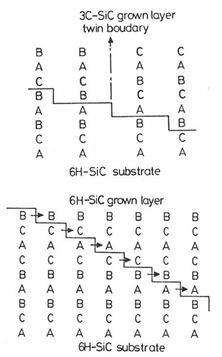
Fig.1(a) shows a typical surface morphology of a grown layer on a natural face. A mosaic pattern with step-like or groove-like boundaries was observed. RHEED and etch pit observations revealed that these layers were twin-crystalline 3C-SiC. Single-crystalline SiC could not be obtained on natural faces, even after varying growth conditions.

(a) natural (0001) face and (b) off-oriented substrates.
In contrast, growth on off-oriented substrates resulted in very smooth surfaces, as shown in Fig. 1(b). RHEED observation confirmed that the grown layers were single-crystalline 6H-SiC. Single crystals were obtained at growth temperatures between 1400 and 1500 °C, which are significantly lower than the conventional growth temperature of 1800 °C.
Figure 2 shows the relationship between polytypes and off-orientation. When the off-angle exceeded 1.5°, homoepitaxial growth of 6H-SiC was achieved. This behavior is explained by the increased density of surface steps, which promotes step-controlled epitaxial growth and inheritance of stacking order at step edges.Fig.3 shows the temperature dependence of the growth rate.
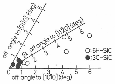
the magnitude and direction of off-orientation.
—————————
*) 3C-SiC has cubic-structure and usually cubic-lattice Miller indices (ex. [hkl]) are used. However to avoid a confusion, in this paper, hexagonal-lattice indices (ex. [a1a2a3c]) are used.
3.2 Fabrication of p–n Junction Diodes
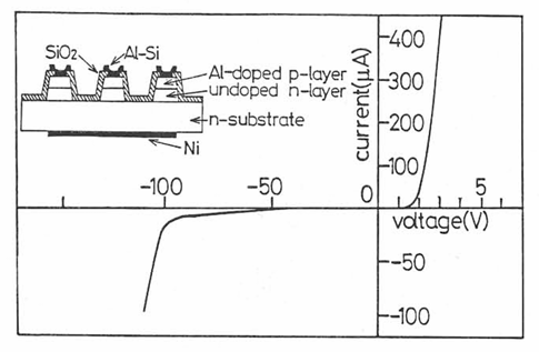
Mesa-type 6H-SiC p–n junction diodes were fabricated using homoepitaxially grown layers. An undoped n-layer and an Al-doped p-layer were grown successively on off-oriented substrates at 1500 °C. Mesa structures were formed by reactive ion etching, followed by thermal oxidation at 1050 °C for surface passivation.
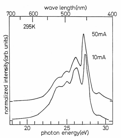
Ohmic contacts were formed using Al–Si for p-type layers and Ni for n-type layers. Fig.4 shows the current–voltage characteristics of a fabricated diode, exhibiting a breakdown voltage of approximately 100 V. Electroluminescence spectra are shown in Fig. 5, where blue-light emission with a peak around 460 nm was observed at room temperature.
4. Conclusion
SiC crystals were grown on 6H-SiC (0001) Si-face substrates at 1350–1500 °C by a CVD method. While twin-crystalline 3C-SiC was obtained on natural faces, single-crystalline 6H-SiC was grown on off-oriented substrates at temperatures 300–400 °C lower than conventional growth temperatures. The change in polytypes was explained by control of surface step density. Fabricated p–n junction diodes exhibited excellent rectification and blue-light emission, demonstrating the usefulness of this growth technique for SiC electronic devices.
References
- H. Matsunami, S. Nishino and H. Ono: IEEE Trans. Electron Devices ED-28 (1981) 1235.
- S. Nishino, J. A. Powell and H. A. Will: Appl. Phys. Lett. 42 (1983) 460.
- S. Nishino, H. Suhara and H. Matsunami: Extended Abstr. 16th Conf. Solid State Devices and Materials, Tokyo, 1983, p.317.
- K. Shibahara, S. Nishino and H. Matsunami: J. Crystal Growth 78 (1986) 538.
- K. Shibahara, S. Nishino and H. Matsunami: Appl. Phys. Lett. 50 (1987) 1888.
- K. Shibahara et al.: Extended Abstr. 18th Int. Conf. Solid State Devices and Materials, Tokyo, 1986, p.717.
- V. J. Jennings, A. Sommer and H. C. Chang: J. Electrochem. Soc. 113 (1966) 728.
- S. Nishino, H. Matsunami and T. Tanaka: J. Crystal Growth 45 (1978) 144.
- H. S. Kong, J. T. Glass and R. F. Davis: Appl. Phys. Lett. 49 (1985) 1074.
- A. Suzuki, H. Matsunami and T. Tanaka: J. Electrochem. Soc. 124 (1977) 2141.
- W. V. Muench and I. Pfaffeneder: J. Appl. Phys. 48 (1977) 1931.
コメント