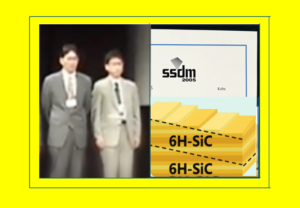
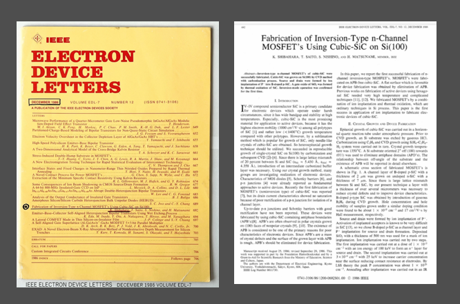
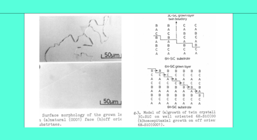
Dr. Kentaro Shibahara was a researcher specializing in semiconductor physics, semiconductor devices, and semiconductor process technologies. During his graduate studies at Kyoto University, he engaged in research on SiC semiconductors and successfully fabricated and demonstrated the world’s first inversion-type SiC-MOSFET. He also developed step-controlled epitaxy, for which he received the SSDM Award.
After engaging in the research and development of highly integrated DRAMs at NEC, he conducted research primarily in silicon semiconductor device physics and advanced scaling process technologies at Hiroshima University. Concurrently, he served in leading roles in major international conferences—including IEDM, the Symposium on VLSI Technology, and SSDM, where he held key positions such as Subcommittee Chair1. Through both these research activities and academic service, he played a leading role in the field and contributed to its advancement. In recognition of these significant contributions, a tribute to his memory was observed during the opening ceremony of the 2011 Symposium on VLSI Technology following his passing.
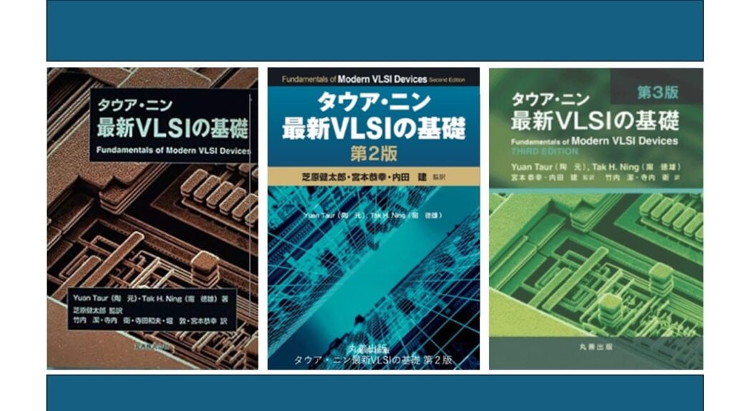
He also contributed to education by supervising the Japanese translation of the standard textbook on advanced CMOS devices, Fundamentals of Modern VLSI Devices by Taur and Ning.
1960 Born in Kobe, Japan 1985 Master’s Degree, Graduate School of Engineering, Kyoto University 1988 Ph.D. in Engineering, Graduate School of Engineering, Kyoto University
Feb 1988 – Jan 1995 NEC Corporation, Japan
Feb 1995 – Apr 2011 Associate Professor, Hiroshima University Research Center for Integrated Systems (from February 1995) Research Center for Nanodevices and Systems (Nanodevice Research Institute) (from May 1995) Research Institute for Nanodevice and Bio Systems (RNBS) (from May 2008) (currently Research Institute for Semiconductor Engineering (RICE))
April 21, 2011 Passed away (Memorial tribute at the 2011 VLSI Symposium opening)